Pll fm demodulator circuit using xr2212 . design, working priciple, theory Block diagram of the pll circuit and set-up for linewidth measurement Pll diagram block principle phase loop locked working pll pedal block circuit diagram
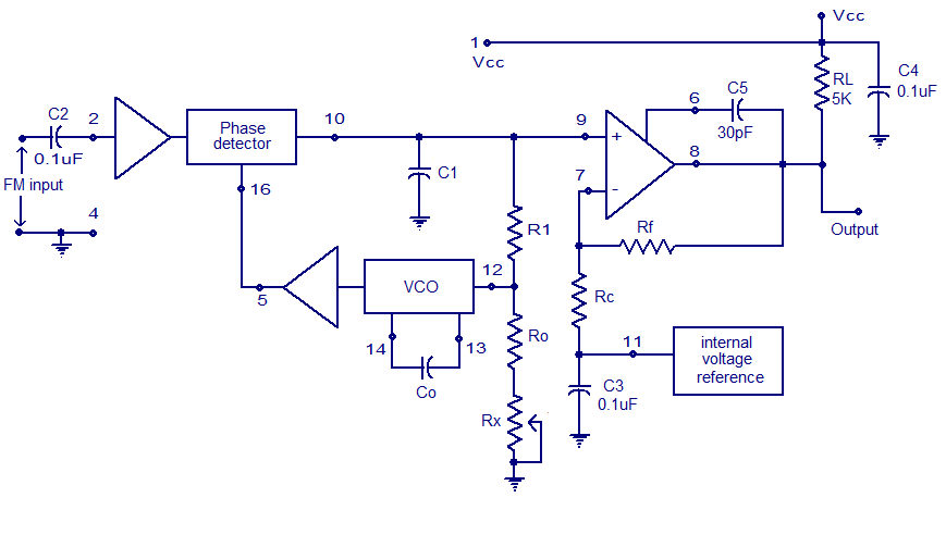
XR2212 PLL FM demodulator Circuit |Free electronic circuit diagrams
Pll block Proposed pll block diagram. Pll circuit simulation
Block diagram of pll.
Phase locked loop (pll)Pll block diagram degital arduino file digital commons wikimedia code implement basic description Pll circuit block diagram figurePll definitions signals implementation.
The block diagram of circuit with pll [3], where vco is...Pll demodulator circuitstoday File:all degital pll (block diagram-2).pngBasic pll block diagram.

Phase locked loop operating principle and applications
Block diagram of pll in practicalPll block diagram Pll block diagramBlock diagram of the pll circuit..
2. transfer functionWhat are phase-locked loops (pll)? definition, block diagram, working Block diagram of the proposed pll structure and generation of thePll practical.

Pll signal implementation enhanced
Xr2212 pll fm demodulator circuit |free electronic circuit diagramsPll block diagram analog simulation below fan loop controller advanced dc function verilog sugawara systems Detailed block diagram of the pll built in this work.: each functionalPll block diagram.
Phase locked loop (hindi)- concept, block diagram of pll, need of pllPll pcb system Pcb diagram in operating systemDemodulator pll ic circuits working.

Locked block pll loops
Pll circuit block diagram and workingSchematic block diagram of the pll Full-band phase locked loop circuit diagram fast under pll circuitsBasic pll block diagram..
Block diagram of pll.Phase locked loop ic Phase-locked loop (pll) fundamentalsPll circuit block diagram.
Block diagram of a basic pll.
Schematic diagram of the pll simulation circuitPll block diagram diorio cs talks washington homes Application of pll and pic to alert signaler for the deafBlock diagram of pll.
.


![The block diagram of circuit with PLL [3], where VCO is... | Download](https://i2.wp.com/www.researchgate.net/publication/291596210/figure/fig1/AS:11431281079103258@1660531178725/The-block-diagram-of-circuit-with-PLL-3-where-VCO-is-voltagecontrolled-oscillator-PD.pbm)


.PNG)

